Creating intricate patterns on metal, glass, or plastic often feels like an impossible balancing act. A medical stent needs 0.1mm-wide channels for drug delivery. A sensor component requires ultra-fine etched lines for conductivity. A decorative glass panel demands detailed designs that stay sharp over time. Traditional methods like stamping or machining struggle with such fine details. They leave burrs, distort thin materials, or simply cannot replicate complex shapes. This is where surface treatment chemical etching excels. By using controlled chemical reactions to remove material, it creates precise, burr-free patterns with exceptional detail. In this guide, we will explore how chemical etching works, its main types, key properties, and how it delivers unmatched precision for both functional and decorative applications.
Introduction
Chemical etching is a versatile surface treatment. It uses chemical reactions to selectively remove material, creating patterns or textures with remarkable precision.
Definition: Chemical etching is a process where a material—metal, glass, or polymer—is exposed to a chemical solution. This solution dissolves unprotected areas, leaving a predefined pattern behind. The process relies on masking: protecting certain areas while allowing the etchant to attack exposed surfaces.
Basic principles: Chemical etching follows four steps:
- Cleaning the substrate to remove contaminants
- Applying a mask (resist) to protect areas from etching
- Exposing the substrate to an etchant solution
- Removing the mask and cleaning the surface
The etchant's strength, temperature, and exposure time control how deep the etching goes.
Industrial significance: Chemical etching is vital for producing microcomponents. These include semiconductor lead frames with 5μm features, medical devices like stents, and aerospace parts such as sensor grids. It is preferred for thin materials (0.01–1mm thick) where mechanical processes would cause deformation.
Environmental considerations: Modern chemical etching prioritizes sustainability. Etchants like ferric chloride are recyclable through filtration systems. These systems remove dissolved metal, reducing waste by 70%. Ventilation systems capture fumes, and neutralization tanks treat wastewater to meet EPA and EU standards.
How Does Chemical Etching Compare to Other Methods?
Different patterning methods offer varying levels of precision, cost, and quality. The table below shows how chemical etching stacks up:
| Feature | Chemical Etching | Laser Etching | Mechanical Machining |
|---|---|---|---|
| Detail Resolution | 5–50 μm | 10–100 μm | 50–500 μm |
| Burr Formation | None | Minimal | Common (needs deburring) |
| Material Thickness | 0.01–1 mm | 0.01–5 mm | 0.1–100 mm |
| Cost for High Volume | Low (reusable masks) | Medium (no masks) | High (tool wear) |
| Complex Shapes | Excellent (3D coverage) | Good (line-of-sight) | Poor (tool access limits) |
A real-world example: a medical device manufacturer needed stainless steel stents with 0.1mm drug-delivery channels. Mechanical machining left burrs that risked tissue damage. Laser etching created heat-affected zones that altered material properties. Chemical etching produced clean, burr-free channels with precise dimensions—and the parts passed regulatory approval on the first attempt.
What Are the Main Types of Chemical Etching?
Chemical etching techniques vary by mask type, etchant, and reaction method. Each type suits specific materials and applications.
Wet Chemical Etching
This type uses liquid etchants in immersion tanks. Common etchants include ferric chloride for metals and hydrofluoric acid for glass. It is ideal for high-volume production of metal parts like shims and filters. Wet etching offers uniform material removal and works well with thin substrates.
Photochemical Etching
This method combines chemical etching with photolithography. A light-sensitive photoresist is applied to the substrate. UV light exposes it through a pattern mask, creating a precise mask after development. This achieves 5–10μm resolution. It is used for semiconductor components, microfluidic chips, and precision sensors.
Electrochemical Etching
This method uses an electric current to speed up the etching reaction. The substrate acts as an anode in an electrolytic cell. The etchant serves as the electrolyte. Electrochemical etching is 2–5 times faster than wet etching. It offers better depth control for aerospace parts and tooling with tight tolerances.
Selective Etching
This type targets specific areas using stencils, tapes, or custom masks. It is ideal for simple patterns like serial numbers or logos. Selective etching offers a cost-effective solution for low-volume runs.
Isotropic Etching
This method removes material uniformly in all directions. It creates rounded edges rather than sharp corners. Isotropic etching works well for decorative metal panels and plastic components where sharp corners are not critical.
Anisotropic Etching
This method etches faster in one direction—such as along crystal planes in silicon. It creates sharp, vertical walls. Anisotropic etching is essential for semiconductor wafers and microelectromechanical systems (MEMS).
What Properties Make Chemically Etched Surfaces Valuable?
Chemically etched surfaces offer a unique combination of precision, finish, and performance.
Detail Resolution
Photochemical etching achieves 5–10μm line widths. That is smaller than a human hair. This enables microscale features like the 10μm channels in medical microfluidic devices. Most mechanical processes cannot match this precision.
Surface Finish
Chemically etched surfaces are smooth with Ra 0.1–0.5μm. They have no burrs because the etchant dissolves material uniformly rather than cutting it. This is critical for medical devices, where rough surfaces could irritate tissue.
Dimensional Accuracy
Etching depth stays within ±1μm. Parts meet tight tolerances, such as 0.05mm thick shims with ±0.001mm variation. This precision prevents performance issues in assemblies with close fits.
Conformal Etching
Chemical etchants reach all exposed surfaces. This includes recesses, holes, and curved areas. Uniform pattern coverage is vital for complex parts like aerospace turbine blades with cooling holes.
Depth Control
Etching depth ranges from 1μm to 1mm. You can adjust it by varying etchant concentration, temperature, and exposure time. For example, 30°C ferric chloride etches 0.01mm of copper per minute, allowing precise depth tuning.
Corrosion Resistance
Properly cleaned etched surfaces resist corrosion as well as unprocessed material. Passivated stainless steel parts etched with nitric acid survive 5000+ hours of salt spray testing (ASTM B117).
Adhesion
Etched surfaces have micro-textures. These improve coating adhesion by 30–50% compared to smooth surfaces. Automotive parts benefit here—paint and plating bond better to etched substrates.
Where Is Chemical Etching Used?
Chemical etching solves diverse challenges across industries. Here are common applications with real-world context.
Aerospace
Etched sensor grids on aircraft wings measure airflow. Lightweight etched panels reduce fuel consumption. Electrochemical etching creates precise cooling holes (0.5mm diameter) in turbine blades with ±0.01mm tolerance.
Medical Devices
Photochemical etching produces stainless steel stents with 0.1mm drug-delivery channels. Titanium implants get porous surfaces that promote bone growth. Etched surgical tools have smooth edges to minimize tissue damage.
Case example: A European medical device company reduced post-processing time by 60% after switching to photochemical etching for surgical instruments. Burr-free edges eliminated manual deburring, and consistent quality reduced inspection rejections.
Electronics
Semiconductor lead frames with 5μm fine lines use photochemical etching. Flexible circuits use wet etching to create conductive pathways on polymer substrates.
Consumer Goods
Decorative metal panels—like smartphone backs and watch cases—use selective etching for logos and patterns. Glassware features etched designs that resist scratching better than printed ones.
Automotive
Etched shims ensure precise spacing in engine assemblies. Fuel injector nozzles with etched micro-holes (0.1mm) improve fuel atomization and efficiency. One Asian automaker reported a 3% fuel efficiency gain after adopting etched injector components.
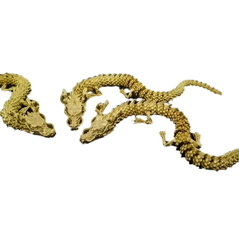
Jewelry
Precious metals like gold and silver are etched to create intricate designs. Photochemical etching enables detailed patterns that rival hand engraving at a fraction of the cost for mass production.
Filtration
Etched metal filters—stainless steel or nickel—have precise pore sizes (10–100μm). These serve industrial and medical applications, from water purification to blood filtering.
What Equipment and Processes Are Involved?
The chemical etching process relies on specialized equipment designed for precision and safety.
Etching Tanks
Tanks are made of chemical-resistant materials like polypropylene or PVC. Sizes range from 10L for laboratory work to 1000L for industrial production. Tanks include heating elements to maintain 20–60°C. Agitation systems—air spargers or mechanical stirrers—ensure uniform etchant distribution.
Chemical Solutions
Etchants are tailored to the substrate:
- Ferric chloride: Copper, steel
- Nitric acid: Aluminum
- Hydrofluoric acid: Glass
- Chromic acid: Polymers
Concentrations range from 10–40% to control etching rate.
Photoresist Materials
These are liquid or dry films that harden when exposed to UV light. Application methods include spraying, dipping, or lamination. Thickness ranges from 1–50μm.
Masks and Stencils
- Laser-cut polymer stencils: For simple patterns
- Photomasks: High-resolution glass plates with chrome patterns for complex designs
Photomasks are reusable for thousands of parts.
Temperature Control
Digital thermostats maintain etchant temperature within ±1°C. A 5°C increase can double the etching rate, risking uneven depth.
Safety Equipment
Operators use acid-resistant gloves (nitrile or neoprene), face shields, and fume hoods with HEPA filters. Emergency eyewash stations and neutralizing kits (sodium bicarbonate) are mandatory for handling corrosive etchants.
Pre-Treatment Processes
Substrates are cleaned with alkaline degreasers, rinsed, and dried. This removes oils and oxides—critical for uniform resist adhesion. Abrasive blasting may improve resist bonding on rough surfaces.
Post-Treatment Processes
Etched parts are rinsed in deionized water. They then dip in neutralizing solutions—like ammonia for acid etchants—to stop the reaction. The resist is stripped with solvents or caustic solutions. Parts are dried in ovens at 60–80°C.
How Do You Ensure Quality and Maintain Equipment?
Rigorous quality control ensures etched parts meet design specifications every time.
Dimensional Inspection
Optical comparators and coordinate measuring machines (CMM) verify pattern dimensions. Tolerances can be as tight as ±5μm for semiconductor components. For microscale features, scanning electron microscopy (SEM) checks line width and spacing.
Depth Measurement
Stylus profilometers and laser confocal microscopes measure etching depth. Consistency stays within ±1μm across batches. This is critical for parts like gaskets, where thickness variation affects sealing.
Surface Inspection
Visual checks under 50–100x magnification identify defects. Look for undercutting (excessive etching under the mask), pinholes, or incomplete etching. Automated vision systems inspect high-volume parts at 1000+ units per hour.
Etchant Analysis
Regular testing—using titration or conductivity—ensures etchant concentration stays within 5% of target. This prevents slow or uneven etching. Spent etchant is recycled or disposed of per hazardous waste regulations.
Equipment Maintenance
Etching tanks are cleaned weekly to remove sludge. Heating elements are calibrated monthly. Mask alignment systems are checked for accuracy to prevent pattern distortion.
Safety Audits
Monthly inspections of fume hoods, PPE, and emergency equipment ensure compliance with OSHA and EU safety standards. Operators receive annual training on chemical handling and spill response.
Quality Standards
Compliance with ISO 9001 (general manufacturing), ISO 13485 (medical devices), and ASTM B809 (chemical etching of metals) ensures reliability. Aerospace parts meet AS9100 for traceability and performance.
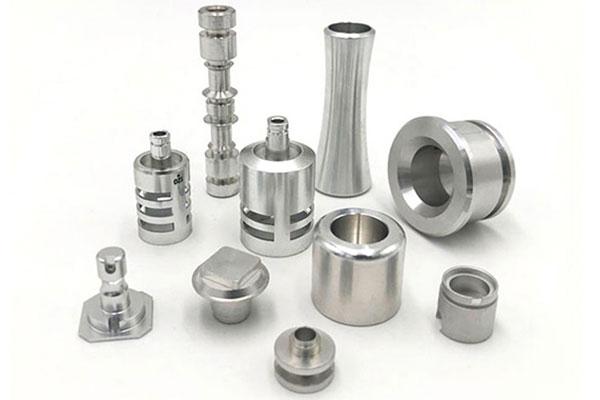
Yigu Technology’s Perspective
As a leading custom manufacturing supplier in China, Yigu Technology specializes in chemical etching for aerospace, medical, and electronics industries. Our capabilities include photochemical etching (5μm resolution), wet etching for metals and glass, and electrochemical etching.
We handle materials from stainless steel and aluminum to silicon and glass. Our automated etching lines use real-time process monitoring. This ensures depth uniformity within ±1μm and defect rates below 0.1%.
Our eco-friendly processes recycle etchants and treat wastewater. We comply with ISO 14001 environmental standards. Our quality lab features SEM and profilometers, enabling precise inspection of even the smallest features.
Whether you need microfluidic chips, aerospace filters, or decorative etched panels, we deliver precision parts on time and within budget—tailored to your specifications.
Conclusion
Chemical etching offers unmatched precision for creating complex patterns on metals, glass, and polymers. It solves the limitations of mechanical machining and laser etching by delivering burr-free surfaces, exceptional detail resolution (down to 5μm), and uniform material removal across complex geometries. From medical stents to aerospace turbine blades, chemical etching provides the accuracy and consistency that critical applications demand. With controllable depth, excellent adhesion properties, and environmentally sustainable processes, it stands as a proven solution for both functional and decorative surface treatments. For manufacturers seeking high-precision patterning without compromising material integrity, chemical etching remains the gold standard.
FAQs
What materials can be chemically etched?
Chemical etching works on most metals (copper, steel, aluminum, titanium), glass, silicon, and some polymers like polyimide and PEEK. Each material requires a specific etchant: ferric chloride for metals, hydrofluoric acid for glass, and oxygen plasma for polymers.
How long does the chemical etching process take?
Etching time depends on depth and material. 0.01mm of copper takes about 1 minute with ferric chloride. 0.1mm of stainless steel takes roughly 10 minutes. Photochemical etching adds mask preparation time (1–2 days) for new designs, but masks are reusable for high-volume runs.
Is chemical etching cost-effective for small production runs?
For small runs (under 1000 parts), chemical etching is cost-effective if using simple stencils. Photochemical etching has higher initial mask costs but becomes economical for medium-to-large runs (over 5000 parts) due to reusable masks and fast processing.
What is the difference between isotropic and anisotropic etching?
Isotropic etching removes material uniformly in all directions, creating rounded edges. It suits decorative applications where sharp corners are not critical. Anisotropic etching removes material faster in one direction—such as along crystal planes in silicon—creating sharp, vertical walls for semiconductor and MEMS applications.
How do you prevent undercutting in chemical etching?
Undercutting occurs when the etchant attacks material beneath the mask. Prevention strategies include: using higher-quality photoresists with better adhesion, optimizing etchant concentration and temperature, reducing etch time, and applying double-sided masking for through-etching applications.
Contact Yigu Technology for Custom Manufacturing
Looking to achieve precision patterns on your metal, glass, or polymer components? Yigu Technology specializes in custom chemical etching solutions tailored to your industry—whether aerospace, medical, electronics, or consumer goods. Our advanced photochemical etching lines, strict quality controls, and experienced engineering team ensure consistent, high-precision results at scale. Contact us today to discuss your project requirements and receive a customized manufacturing proposal.