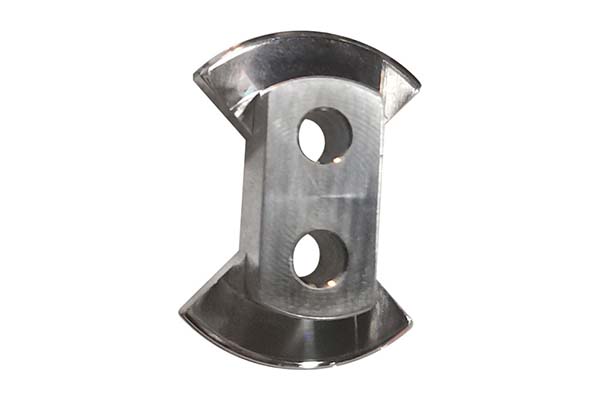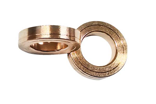
If you need a material that combines extreme strength, electrical conductivity, and corrosion resistance, you face a tough choice. Most high-strength alloys sacrifice conductivity. Pure copper offers excellent conductivity but lacks durability. Metal Stamping C17200 (Beryllium Copper) solves this dilemma. It delivers tensile strength exceeding 1,200 MPa and electrical conductivity up to 45% IACS—a rare combination. However, stamping this alloy requires specialized expertise to manage its heat treatment needs and avoid brittleness. This guide covers its properties, stamping process, applications, and quality standards to help you produce reliable, high-performance components.
What Makes C17200 Beryllium Copper Unique?
Composition and Mechanical Properties
C17200’s exceptional performance comes from its precise alloy makeup. It consists of 97.7–98.5% copper, 1.6–2.0% beryllium, and trace amounts of nickel.
| Property | Value | Significance |
|---|---|---|
| Tensile Strength | 690 MPa (annealed) to 1,240 MPa (heat-treated) | Outperforms most stainless steels while remaining formable |
| Electrical Conductivity | 25–45% IACS | Balances strength with electrical performance |
| Hardness | 38–42 HRC (heat-treated) | Comparable to tool steel; ensures wear resistance |
| Corrosion Resistance | Superior to most copper alloys | Resists saltwater, industrial chemicals, and tarnishing |
| Thermal Stability | Maintains properties up to 200°C | Prevents degradation in high-heat applications |
These properties make C17200 the material of choice for parts where failure is not an option—aerospace sensors, medical devices, and critical electrical contacts.
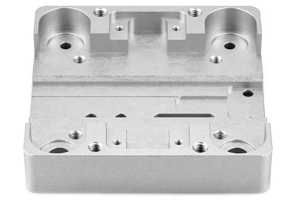
How Do You Stamp C17200 Beryllium Copper?
A Two-Step Process: Form Then Strengthen
Stamping C17200 requires a strategic approach. The alloy is typically stamped in its annealed state (soft temper) for maximum formability, then heat-treated to achieve full strength. This two-step process avoids cracking during forming.
Die Design
Use carbide dies with polished surfaces (Ra ≤ 0.2 μm) to prevent galling. C17200’s hardness can accelerate tool wear. Maintain punch-die clearance of 8–10% of material thickness to ensure clean edges.
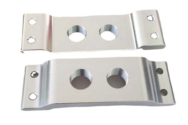
Blanking and Forming
- Blanking: Requires high-pressure presses—300–500 tons—to handle annealed C17200’s toughness.
- Forming: Use gradual bends with a minimum radius of 1× material thickness to avoid surface defects.
Heat Treatment
After stamping, the material undergoes two steps:
- Solution Anneal: Heat to 780–820°C for 30 minutes, then quench in water.
- Age Hardening: Heat to 315–330°C for 2–4 hours.
This process precipitates beryllium-copper compounds, increasing strength by 60–80%.
Surface Finishing
Electroplating with gold or nickel enhances conductivity and corrosion resistance. This is critical for electrical contacts in harsh environments.
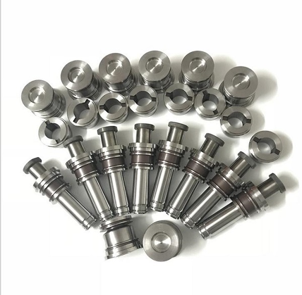
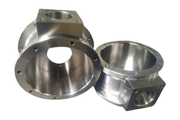
Where Is C17200 Beryllium Copper Used?
Critical Applications Across Industries
C17200’s unique blend of properties makes it indispensable in high-performance sectors.
| Industry | Application | Why C17200 Works |
|---|---|---|
| Aerospace | Landing gear sensors, avionics | Combines strength, conductivity, and corrosion resistance under strict safety standards |
| Electrical | Connectors, switches, relays | Ensures reliable signal transmission with low resistance and durability |
| Automotive | Battery contacts, valve springs | Withstands millions of cycles without fatigue |
| Medical | Surgical instruments, diagnostic equipment | Offers precision, corrosion resistance, and biocompatibility |
| Electronics | Smartphone antennas, computer connectors | Balances miniaturization with performance |
| Tooling | Precision molds for plastic injection | Leverages high hardness and thermal conductivity for consistent cooling |
Each application relies on C17200’s ability to perform under extreme stress, temperature, and corrosive conditions.
What Quality Standards Apply?
Testing and Certification for Reliability
Maintaining C17200’s performance requires adherence to strict standards.
| Standard | Purpose |
|---|---|
| ASTM B194 | Specifies chemical composition and mechanical properties; requires minimum 1,035 MPa tensile strength after heat treatment |
| ISO 13373 | Outlines testing procedures for beryllium copper, including conductivity and hardness measurements |
Testing Requirements
- Tensile Tests: Verify strength on heat-treated samples.
- Conductivity Tests: Use eddy current testing to confirm ≥25% IACS for electrical applications.
- Dimensional Accuracy: Maintain tolerances of ±0.005 mm for critical features like contact points using CMMs.
- Surface Finish: Require Ra ≤ 0.4 μm to prevent electrical arcing and reduce wear in moving parts.
Conclusion
C17200 beryllium copper offers a rare combination of high strength, electrical conductivity, and corrosion resistance. Its tensile strength reaches 1,240 MPa after heat treatment, while conductivity hits 45% IACS. The stamping process requires forming the material in its annealed state, then heat-treating to achieve full strength. Use carbide dies, maintain tight clearances, and follow precise heat treatment cycles. Quality control includes tensile testing, conductivity verification, and strict dimensional checks. When processed correctly, C17200 delivers reliable performance in aerospace, electrical, automotive, and medical applications.
FAQ
How does C17200 compare to phosphor bronze for springs?
C17200 offers 30–40% higher tensile strength and better electrical conductivity. However, it costs 2–3 times more. Use C17200 for high-stress, high-conductivity applications. Choose phosphor bronze for cost-sensitive uses where conductivity requirements are lower.
Is beryllium copper safe to stamp?
Yes, with proper handling. Beryllium dust is toxic, so use ventilation systems and avoid dry grinding or sanding. Stamping in the annealed state generates less dust. Always follow workplace safety guidelines for beryllium-containing materials.
What is the maximum thickness for stamping C17200?
C17200 is practical for sheets up to 1.5 mm thick. For thicker material—1.5–3 mm—pre-annealing and slower press speeds are required to prevent cracking during forming.
Why does C17200 need heat treatment after stamping?
Heat treatment, specifically solution annealing followed by age hardening, increases strength by 60–80%. Stamping in the annealed state allows complex forming without cracking. The subsequent heat treatment precipitates beryllium-copper compounds, achieving the final mechanical properties.
What surface finish is best for C17200 electrical contacts?
For electrical contacts, gold plating over a nickel underlayer provides low contact resistance and excellent corrosion protection. A surface finish of Ra ≤ 0.4 μm prevents arcing and ensures consistent performance over millions of cycles.
Contact Yigu Technology for Custom Manufacturing
Stamping C17200 beryllium copper requires precision, controlled heat treatment, and rigorous testing. At Yigu Technology, we specialize in custom stamping of beryllium copper for aerospace, medical, and electrical clients. We control the entire process—from annealing to heat treatment—to ensure parts meet ASTM B194 standards.
Our quality system includes tensile testing, conductivity verification, and dimensional inspections. Whether you need connectors, springs, or precision contacts, we deliver components that perform reliably in critical applications.
Contact Yigu Technology today to discuss your C17200 stamping project.