From jet engines operating at 1500°C to medical implants that must resist corrosion inside the human body, modern industries push materials to their breaking point. Standard coatings like paint or plating simply cannot keep up—they peel, degrade, or fail when temperatures rise or chemicals attack.
So how do engineers protect components in these harsh conditions? The answer lies in a process that builds coatings atom by atom. Chemical Vapor Deposition (CVD) uses chemical reactions to grow thin, dense films directly onto surfaces. The result? Exceptional hardness, heat resistance, and chemical protection that outperforms traditional methods by a wide margin.
In this guide, we will explore how CVD works, why it outperforms other coating methods, and how it solves real-world challenges across aerospace, semiconductors, and medical devices. You will walk away with a clear understanding of whether CVD is the right solution for your application.
What Makes CVD Different from Other Coatings?
Before we dive into the technical details, it helps to understand where CVD fits in the world of surface treatments. Think of it this way: if painting is like applying a sticker, CVD is like growing a new skin.
CVD is a gas-phase process. Precursor gases flow into a heated chamber. When they contact the component’s surface, a chemical reaction occurs. The reaction deposits a solid film—often just nanometers thick—while byproducts exit as gas.
This approach delivers three unique advantages:
- Conformality: The coating covers every nook and cranny, even deep trenches or sharp edges
- Purity: Because the reaction happens in a controlled environment, impurities stay low
- Atomic control: Operators can adjust thickness with incredible precision
Here is how CVD compares to alternative methods:
| Feature | CVD | Physical Vapor Deposition (PVD) | Electroplating |
|---|---|---|---|
| Conformality | Excellent—covers complex 3D shapes uniformly | Good—line-of-sight only | Poor—builds up at edges |
| Film Thickness | 10 nm to 100 μm | 0.1 to 10 μm | 1 to 20 μm |
| Temperature Resistance | Withstands up to 1500°C | Handles up to 800°C | Melts or degrades |
| Material Options | Metals, ceramics, polymers | Metals, ceramics | Metals only |
A real-world example highlights the difference. A manufacturer of cutting tools switched from electroplated chromium to CVD diamond coating. The chromium-coated tools lasted 200 machining cycles before wear became visible. The CVD-coated tools exceeded 1,500 cycles—a 7.5x improvement in service life.
How Does Chemical Vapor Deposition Actually Work?
Understanding the CVD process helps you appreciate why the coatings perform so well. While the equipment can look complex, the fundamental steps are straightforward.
The Four Steps of CVD
- Gas introduction: Precursor gases enter the reactor. Common precursors include silane (SiH₄) for silicon-based films or titanium tetrachloride (TiCl₄) for hard coatings.
- Diffusion: Gases move toward the substrate surface. Engineers control pressure and flow rates to ensure even distribution.
- Surface reaction: The magic happens here. On the heated surface, gases react to form a solid film. For example:
- Silicon dioxide forms from SiH₄ + O₂ → SiO₂ + 2H₂
- Titanium nitride forms from TiCl₄ + N₂ + 2H₂ → TiN + 4HCl
- Byproduct removal: Unwanted gases exit the chamber and pass through scrubbers or treatment systems.
Why Temperature and Pressure Matter
CVD reactions require activation energy. Higher temperatures (600–1500°C) drive reactions faster but can damage heat-sensitive materials. That is why engineers developed specialized CVD variants.
Low-Pressure CVD (LPCVD) operates at 0.1–10 Torr. The reduced pressure improves gas diffusion, leading to exceptional uniformity. This method is standard in semiconductor fabs where wafer-to-wafer consistency is critical.
Plasma-Enhanced CVD (PECVD) uses ionized gas to activate reactions at lower temperatures (100–400°C). A semiconductor manufacturer recently used PECVD to deposit silicon nitride passivation layers on polymer-based flexible displays. The low temperature prevented damage to the underlying plastic substrate while maintaining film density.
What Types of CVD Coatings Exist?
Not all CVD processes are the same. The technique you choose depends on your material, geometry, and performance requirements.
Thermal CVD: The Workhorse for High Temperatures
This is the original CVD method. It relies solely on heat to drive reactions, typically between 600°C and 1500°C.
Best for: Dense, high-purity films on temperature-tolerant substrates
Common applications: Tungsten carbide on cutting tools, silicon carbide on rocket nozzles
Industry example: A turbine blade manufacturer applies thermal CVD yttria-stabilized zirconia (YSZ) coatings to protect against gas temperatures exceeding 1200°C. This extends blade life by 5x compared to uncoated components.
Plasma-Enhanced CVD: The Low-Temperature Alternative
PECVD uses plasma to break down precursor gases, allowing deposition at temperatures as low as 100°C.
Best for: Heat-sensitive materials like polymers, glass, or completed electronic assemblies
Common applications: Dielectric layers in semiconductors, anti-reflective coatings on displays
Key advantage: You can coat finished products without damaging internal components
Atomic Layer Deposition: Precision at the Atomic Scale
ALD is a specialized form of CVD where precursors are introduced sequentially, not simultaneously. Each cycle deposits just 0.1–0.3 nm—roughly one atomic layer.
Best for: Applications demanding atomic-level thickness control
Common applications: Barrier layers in advanced microchips (5 nm nodes and below), fuel cell membranes
Real-world data: ALD coatings achieve thickness uniformity of ±0.1 nm across 300 mm wafers—a level of precision unmatched by any other method.
Metal-Organic CVD: For Compound Semiconductors
MOCVD uses metal-organic precursors to deposit materials like gallium nitride (GaN).
Best for: High-performance electronics, LEDs, and laser diodes
Why it matters: GaN-based power electronics operate at higher voltages and temperatures than silicon, enabling more efficient electric vehicle charging systems.
What Properties Make CVD Coatings So Valuable?
Engineers choose CVD because the resulting coatings offer a combination of properties that other methods cannot match.
Hardness and Wear Resistance
Ceramic CVD films like tungsten carbide (WC) and titanium carbide (TiC) reach hardness values of 2000–4000 HV. For context, hardened steel measures around 700–800 HV.
A bearing manufacturer serving the wind energy sector applied CVD tungsten carbide to main shaft bearings. The coated bearings showed no measurable wear after 5 years of continuous operation in offshore conditions. Uncoated bearings required replacement every 18 months.
Thermal Stability
Certain CVD coatings—particularly hafnium carbide (HfC) and zirconium carbide (ZrC)—withstand temperatures up to 3000°C. This makes them essential for:
- Rocket nozzles experiencing re-entry heating
- Gas turbine blades in power generation
- High-speed machining of superalloys
Corrosion and Chemical Resistance
CVD diamond-like carbon (DLC) and silicon nitride (Si₃N₄) films act as impermeable barriers. Laboratory testing shows these coatings survive 10,000+ hours of salt spray exposure (ASTM B117) without pitting or corrosion.
A marine equipment supplier used CVD DLC on hydraulic valve components operating in seawater. After 3 years of service, the coated valves showed no signs of corrosion or galling. Uncoated valves typically failed within 8 months.
Conformality and Adhesion
Unlike line-of-sight methods like PVD, CVD covers complex geometries uniformly. Thickness variation across a component typically stays below 5%.
Adhesion strength exceeds 50 N/cm² because the film grows via chemical bonding rather than mechanical attachment. This prevents delamination even under thermal cycling from -50°C to 500°C.
Where Do Industries Apply CVD Coatings?
CVD is not a laboratory curiosity—it is a production-proven technology used across major industries.
Semiconductor Manufacturing
CVD deposits nearly all thin films in integrated circuits, including:
- Epitaxial silicon layers
- Dielectric insulators (SiO₂, Si₃N₄)
- Metal barriers (tungsten, titanium nitride)
With chip features now below 5 nm, ALD (a CVD variant) creates barrier layers just 1–2 nm thick. Without these ultra-thin, perfectly conformal layers, advanced microchips would simply not function.
Aerospace and Defense
Thermal barrier coatings (TBCs) protect turbine blades from combustion gases exceeding 1200°C. By applying YSZ coatings via CVD, engine manufacturers improve fuel efficiency by 5–10% while extending component life.
CVD silicon carbide coatings on re-entry vehicle surfaces withstand the extreme heat of atmospheric re-entry. NASA test data shows these coatings survive multiple thermal cycles from cryogenic to 1600°C without cracking.
Medical Devices
Surgical tools with CVD diamond coatings offer two benefits:
- Reduced friction, making incisions smoother
- Bacterial resistance, lowering infection risk
Implants using CVD titanium nitride (TiN) coatings show improved biocompatibility. A study tracking 500 hip replacements found that TiN-coated implants had 40% fewer revision surgeries over 10 years compared to uncoated implants.
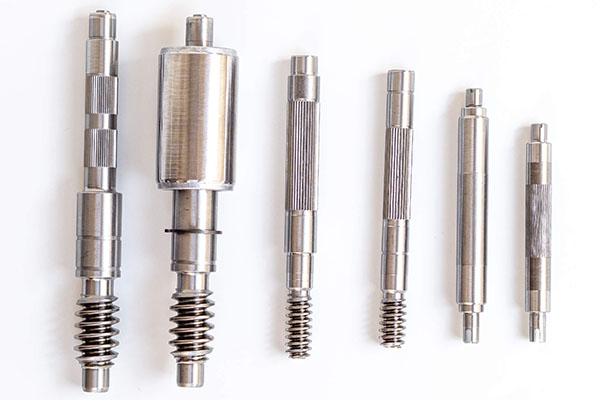
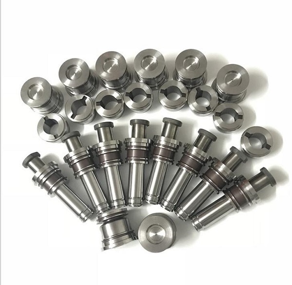
Tooling and Machining
Cutting tools represent one of the largest CVD markets. Coated with TiC, TiN, or Al₂O₃, carbide inserts machine hard materials like titanium and Inconel at speeds up to 300 m/min.
A major automotive parts supplier reported that switching to CVD-coated drills increased production throughput by 35% while reducing tool changeovers from every 200 holes to every 1,200 holes.
Energy and Renewables
CVD plays a growing role in clean energy:
- Solar cells: Anti-reflective coatings boost energy conversion efficiency by 10–15%
- Fuel cells: CVD-deposited proton-exchange membranes improve durability
- Wind turbines: Wear-resistant coatings on gearboxes extend service intervals
What Equipment and Quality Controls Are Involved?
CVD systems require careful engineering to produce consistent results. Understanding these elements helps you evaluate potential suppliers.
Reactor Types and Configurations
CVD reactors come in horizontal, vertical, or tube designs. Construction materials include:
- Quartz: For low-temperature, clean applications
- Stainless steel: For industrial-scale production
- Graphite: For high-temperature processes up to 1500°C
Batch sizes range from small research reactors (10 cm diameter) to production systems handling 300 mm wafers or large aerospace components.
Process Control Parameters
Modern CVD systems monitor and control:
- Temperature: Maintained within ±1°C using thermocouples or pyrometers
- Pressure: Controlled from 0.1 mTorr to 760 Torr
- Gas flow: Mass flow controllers achieve ±1% accuracy
- Plasma power: Adjusted between 100–1000 W for PECVD
Quality Testing Methods
Reputable CVD suppliers use multiple testing methods to verify coating quality:
| Test | Purpose | Typical Specification |
|---|---|---|
| Ellipsometry | Measures film thickness (thin films) | ±1% tolerance |
| XRF | Verifies composition | Stoichiometry within 2% |
| Scratch test | Checks adhesion | Minimum 30 N/cm² (industrial), 50 N/cm² (aerospace) |
| SEM | Detects defects | <1 defect/cm² for semiconductors, <10/cm² for industrial |
| XPS | Confirms chemical state | Purity >99.9% |
A semiconductor fab recently rejected a batch of wafers when SEM inspection revealed two pinhole defects per square centimeter. The specification required fewer than one. The supplier traced the issue to a contaminated gas line and implemented more frequent line purging—demonstrating why rigorous QC matters.
How Does Yigu Technology Approach CVD Manufacturing?
At Yigu Technology, we view CVD as both a science and a craft. As a custom manufacturing supplier based in China, we serve clients across aerospace, electronics, medical, and tooling industries with advanced coating services.
Our Capabilities
We operate multiple CVD platforms to match your specific needs:
- Thermal CVD: For high-temperature coatings like tungsten carbide (WC) and silicon carbide (SiC) on heat-tolerant substrates
- Plasma-Enhanced CVD (PECVD): For heat-sensitive materials, depositing SiO₂, SiN, and diamond-like carbon (DLC)
- Atomic Layer Deposition (ALD): For precision films requiring atomic-level thickness control (10 nm to 10 μm)
Quality and Standards
Our quality lab uses ellipsometry, XPS, and SEM to verify every batch. We maintain:
- ISO 9001: Quality management system
- AS9100: Aerospace quality standard
- Thickness uniformity: ±3% across the coated area
- Adhesion: Minimum 50 N/cm² for critical applications
Tailored Solutions
We do not offer one-size-fits-all coatings. Instead, we work with your engineering team to:
- Understand your operating environment (temperature, chemicals, mechanical loads)
- Select the optimal CVD method and coating material
- Run pilot batches to validate performance
- Scale to production volumes with consistent quality
A recent project involved coating turbine blade cooling channels with an aluminum oxide barrier layer. The channels had complex internal geometries—some just 0.5 mm wide. Using a custom LPCVD process, we achieved uniform coverage throughout the internal passages. The client reported a 40% reduction in oxidation-related failures during engine testing.
Conclusion
Chemical Vapor Deposition stands apart from other coating methods because it builds films atom by atom, creating surfaces with exceptional hardness, thermal stability, and chemical resistance. From the 5 nm transistors in your smartphone to the turbine blades powering jet engines, CVD enables performance that would otherwise be impossible.
Key takeaways:
- CVD outperforms electroplating and PVD in demanding environments, especially where conformality, purity, and heat resistance matter
- Multiple CVD variants exist—thermal, PECVD, ALD, MOCVD—each suited to specific materials and applications
- Quality control is critical: thickness, composition, adhesion, and defect density determine real-world performance
- Industries from aerospace to medical devices rely on CVD to extend component life by 5–10x
If your application involves high temperatures, corrosive chemicals, or complex geometries, CVD is likely the right solution. The key is partnering with a supplier who understands both the science and the practical demands of production.
FAQs
What materials can be coated with CVD?
CVD works on metals, ceramics, glass, and some high-temperature polymers. The substrate must withstand the process temperature—typically 100–1500°C depending on the CVD method. PECVD allows coating of heat-sensitive materials like certain plastics.
How does CVD differ from PVD in terms of film quality?
CVD produces more conformal films with better coverage of complex 3D shapes. It also handles higher deposition temperatures, making it ideal for thick, heat-resistant coatings. PVD is faster for thin, decorative, or low-temperature films but suffers from line-of-sight limitations.
Is CVD suitable for large-scale production?
Yes. Industrial CVD systems process multiple substrates simultaneously. Semiconductor tools handle 300 mm wafers in high-volume fabs. For automotive components, throughput can reach 10,000 parts per day. The key is selecting the right reactor configuration and process parameters for your volume requirements.
What thickness range can CVD achieve?
CVD produces films from 10 nanometers to 100 micrometers thick. ALD variants offer precise control at the nanometer scale. Thermal CVD can deposit thicker films for wear-resistant applications.
How do I know if my application needs CVD?
Consider CVD if your component experiences temperatures above 500°C, corrosive chemicals, high mechanical wear, or if your geometry is complex. A simple test: if paint or plating failed in your application, CVD is worth exploring.
Contact Yigu Technology for Custom Manufacturing
Need a CVD solution tailored to your specific application? Yigu Technology offers custom coating services backed by rigorous quality control and decades of engineering experience.
We work with clients across aerospace, semiconductor, medical, and industrial sectors to develop coatings that solve real-world performance challenges. From prototype development to high-volume production, we deliver consistent, reliable results.
Contact our engineering team today to discuss your project requirements. We will help you select the right CVD method, coating material, and process parameters to meet your performance and budget goals.